notes for class 12 physics chapter 14: semiconductor electronics, materials, devices and sample circuits download pdf, semiconductor electronics materials, devices and simple circuits 12 notes, class 12 physics notes, semiconductor electronics materials, devices and simple circuits class 12, semiconductor electronics materials, devices and simple circuits class 12 notes, class 12 semiconductor electronics materials, devices and simple circuits, note physics, physics notes, semiconductor electronics materials, devices and simple circuits, class 12 cphysics chapter 14 notes, 12th standard physics notes, 12th std physics notes, class 12 physics notes chapter 14, semiconductor electronics materials, devices and simple circuits chapter class 12 notes
It is the branch of science which deals with the electron flow through a vacuum, gas or semiconductor.
Classification of substances on the basis of conduction of electricity.
We know that, each substance is composed of atoms. Substances are mainly classified into three categories namely solids, liquids and gases.
In each solid atoms are at a definite positions and the average distance between them is constant. Depending upon the internal arrangement of atoms, solids are further divided into two groups.
The solid in which the atoms are arranged in a regular order are called the crystalline solids. In other words, we can say that in a crystalline solid.there is periodicity and regularity of its component atoms in all the directions. For example sodium chloride (common salt), diamond, Sugar, silver etc are the crystalline solids.
Their atoms are arranged in a definite geometrical shape.
They have a definite melting point.
They are anisotropic, i.e., their physical properties such as thermal Conductivity refractive index etc, are different in different directions.
They are the real solids.
The Solids in which the atoms do not have a definite arrangement are called the amorphous solids. They are also called the glassy solids. For example glass, rubber, plastic, power, etc are the amorphous solids.
Tbey do not have a definite arrangement of its atoms, i e., they do not have a characteristic geometrical shape.
They do not have a definite melting point.
They are isotropic. i.e., their physical properties such as conductivity of heat refractive index etc, are same in all the directions.
They are not the real solids.
Monocrystal is a crystal in which the ordered arrangements of the atoms or molecules extends throughout the piece of solid, irrespective of its size.
Polycrystal is a crystalline solid in which each piece of the solid has a number of monocrystals with developed faces joined together.
The polycrystal ceramic made from PbO, ZnO and TiO are used in gas lighters and telephone receivers.
Some organic crystalline solid. when heated acquire fluidity but retain their anisotropic properties. They axe called liquid crystals.
Some liquid crystals like cyanobiphenyl can change the plane of polarization of light and such Liquid Crystal Displays (LCD) are used in watches and micro calculators.
A crystal is made up of a three- dimensional array of points such that each point is surrounded by the height bouring POints in an identical way. Such an array of points is known as bravais lattice or space lattice.
Unit cell is the smallest unit of the crystal lattice, repetition of which in three dimensions gives rise to crystal lattice.
The length of three sides of a unit cell are called Primitives or lattice constant represented by a, b, c. The angle between three crystallographic axis are called interfacial anglesrepresented by α, β and γ. The primitives and interfacial angles constitute the lattice parameters of a unit cell.
[The cubic crystal may be of the form, simple cubic (sc) lattice, the body centred cubic (bee) lattice, the face centred Cubic (fcc) lattice.]
The coordination number is defined as the number of nearest neighbours around any lattice point (or atom) in the crystal lattice.
(a) For sc, coordination number is 6.
(b) For bee, coordination number is 8.
(c) For fcc, coordination number is 12.
(d) For sc, atomic radius is a / 2.
(e) For bcc, atomic is a √3 / 4.
(f) For fcc. atomic radius is a / 2√2.
Conductors are those substances through which electricity can pass easily, e.g., all metals are conductors.
Insulators are those substances through which electricity cannot pass, e.g., wood. rubber, mica etc.
Semiconductors are those substances whose conductivity lies between conductors and insulators. e.g., germanium, silicon, carbon etc.
In a crystal due to interatomic interaction valence electrons of one atom are shared by more than one atom in the crystal. Now splitting of energy levels takes place. The collection of these closely spaced energy levels is called an energy band.
This energy band contains valence electrons. This band may be PartIally or completely filled with electrons but never be empty. The electrons in this band are not capable of gaining nergy from external electric field to take part in conduction of current.
This band contains conduction electrons. This band is either empty or Partially filled with electrons.
Electrons present in this band take part in the conduction of current.
This band is completely empty. The minimum energy required to shift an electron from valence band to conduction band is called band gap (Eg).
Thermionic emission occurs when a metal is heated to a high temperature, the free electrons in the metal gain kinetic energy sufficient to escape through the surface of the metal.
The thermionic diode is a two electrode (cathode and plate) device based on thermionic emission.
A diode allows unidirectional flow of electrons, i.e., only when the plate is positive with respect to cathode. Hence, it is also called a valve.
The triode value consists of three electrodes, e.g., cathode. plate and grid enclosed in an evacuated glass bulb.
Grid influences the space charge and controls the flow of plate current.
[When the grid is given a negative potential with respect to cathode. It repels the electrons escaping from the cathode and Increases the effect of space charge, at sufficientLy negative grid potential is known as cut-off grid bias.
If the grid is given a positive potential with respect to cathode, it attracts the electrons and decreases the effect of space charge. The increasing the plate current. In this case a current flow into the circuit, thus grid modifies the function of valve.]
Grid is always kept at small negative potential with respect to cathode.
Triode can be used as an amplifier, oscillator modulator and demodulator.
An oscillator is an electronic device which generates AC voltage froID DC power. It is basically a positive feedback amplifier with infinite voltage gain.
A semiconductor in its pure state is called intrinsic semiconductor.
A semiconductor doped with suitable impurity to increase its impurity, is called extrinsic semiconductor.
On the basis of doped impurity extrinsic semiconductors are of two types
Extrinsic semiconductor doped with pentavalent impurity like As, Sb, Bi, etc in which negatively charged electrons works as charge carrier, is called n-type semiconductor.
Every pentavalent impurity atom donate one electron in the crystal, therefore it is called a doner atom
Extrinsic semiconductor doped with trivalent impurity like Al, B, etc, in which positively charged holes works as charge carriers, is called p-type semiconductor.
Every trivalent impurity atom have a tendency to accept one electron, therefore it is called an acceptor atom.
In a doped semiconductor ne nh = n2 i where ne and nh are the number density of electrons and holes and ni is number density of intrinsic carriers, i.e., electrons or holes.
In n-type semiconductor, ne > > nh
In p -type semiconductor, nh > > ne
Electrical conductivity of extrinsic semiconductor is given by σ = 1 / ρ = e (ne μe + nh μh)
where ρ is resistivity, μe and μh are mobility of electrons and holes respectively.
Note Energy gap for Ge is 0.72 eV and for Si it is 1.1 eV.
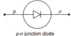
An arrangement consisting a p -type semiconductor brought into a close contact with n-type semiconductor, is called a p -n junction.
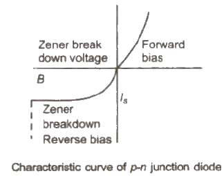
The current in a p-n junction is given by
kB = Io (eeV/k BT – 1 )
where Io is reverse saturation current, V is potential difference across the diode, and kB is the Boltzmann constant.
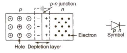
At p-n. junction a region is created, where there is no charge carriers. This region is called depletion layer. The width of this region is of the order of 106 m.
The potential difference across the depletion layer is called potential barrier.
Barrier potential for Ge is 0.3 V and for Si is 0.7 V.
In this biasing, the p -side is connected to positive terminal and n-side to negative terminal of a battery.
In this biasing, forward current flows due to majority charge carriers.
The width of depletion layer decreases.
In this biasing, the p-side is connected to negative terminal and n-side to positive terminal of a battery.
In this biasing, reverse current flows due to minority charge carriers.
The width of depletion layer increases.
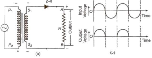
A p-n junction diode can be utilized as a rectifier.
Zener diode, photo-diode, light-emitting diode, etc are specially designed p-n. junction diodes.
The current through p-n junction flow only from p toward n and not from n toward p.
The maximum voltage that a junction diode can bear without break is called zener voltage and the junction diodes possessing this voltage is known as zener diode.
Resistance of diode R = V / I
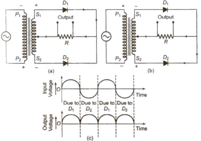
A device which convert alternating current or voltage into direct current or voltage IS known as rectifier. The process of converting AC into DC IS caned rectification.
A half-wave rectifier converts the half cycle of applied AC signal into DC signal. Ordinary transformer may be used here.
A full-wave rectifier converts the whole cycle of applied AC signal into DC signal. Centre top,transformer is used here.
[Half-wave rectifier converts only one-half of AC Into DC while full wave rectifier rectifies both halves of AC input.]
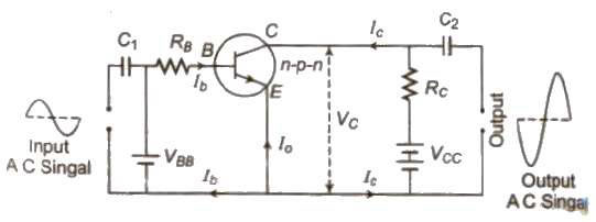
A transistor is an arrangement obtained by growing a thin layer of one type of semiconductor between two thick layers of other similar type semiconductor.
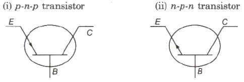
• The left side semiconductor is called emitter, the right side semiconductor is called
collector and the thin middle layer is called base.
• Emitter is highly doped and base is feebly doped.
• A transistor can be utilized as an amplifier and oscillator but not a rectifier
• Maximum amplification is obtained in common-emitter configuration.
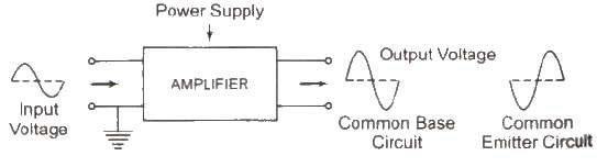
An amplifier is a device which is used for increasing the amplitude of variation of alternating voltage 01′ current or power.
The amplifier thus produces an enlarged version of the input signal.
The general concept of amplification is represented in figure. There are two input terminals for the signal to be amplified and two output terminals for connecting the load; and’ a means of supplying power to the amplifier.
AC current gain (αAC) = ΔIc / ΔIe
where ΔIc is change in collector current and ΔIe change in emitter current.
AC voltage gain (AV) = Output voltage / Input voltage
= αAC * Resistance gain = αAC * Ro / Ri
where Ro is output resistance of the circuit and Ri is input resistance of the circuit.
AC power gain = Change in output power / Change in input power
= AC voltage gain * AC current gain
= α2AC * resistance gain
The input and output signals are in the same phase.
There is no amplification in current of a given signal.
There is an amplification in voltage and power of the given signal.
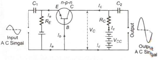
2. In Common Emitter Amplifier
AC current gain (&betaAC) = ΔIc / ΔIe
where ΔIc is change in collector current and ΔIe change in base current.
AC voltage gain (AV) = &beta AC * resistance gain
AC power gain =&beta2AC * Resistance gain
Relation between the current gai n of common base and common emitter amplifier.
β = α / 1 – α = Ic / Ie
The input and output signals are out of phase by π or 180°
There is amplification in current, voltage and power of the given signal.
It is forward biased p-ri junction diode which emits light when recombination of electrons and holes takes place at the junction.
If the semiconducting material of p-ri junction is transparent to light, the light is emitting and the junction becomes a light source, i.e., Light Emitting Diode (LED).
The colour of the light depends upon the types of material used in making the semiconductor diode.
(i) Gallium – Arsenide (Ga-As) – Infrared radiation
(ii) Gallium – phosphide (GaP) – Red or green light
(iii) Gallium – Arsenide – phosphide (GaAsP) – Red or yellow light
A digital circuit which allows a signal to pass through it, only when few logical relations are satisfied, is called a logic gate.
A table which shows all possible input and output combinations is called a truth table.
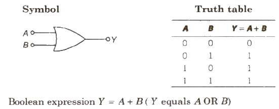
(i) OR Gate It is a two input and one output logic gate.
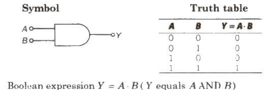
(ii) AND Gate It is a two input and one output logic gate
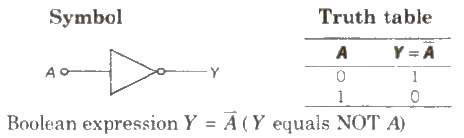
(iii) NOT Gate It is a one input and one output logic gate.
(i) NAND Gate When output of AND gate is applied as input to a NOT gate, then it is called a NAND gate.
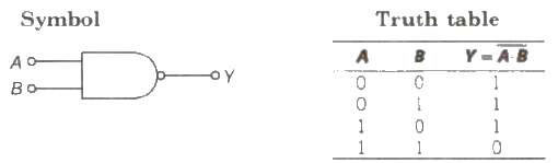
Boolean expression Y = A * B (Y equals negated of A AND B)
(ii) NOR Gate When output of OR gate is applied as input to a NOT gate, then it is called a NOR gate.
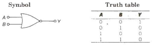
Boolean expression Y = A + B ( Y equals negated of A OR B)
• The Boolean expression obey commutative law associative law as well as distributive
law.
1. A + B = B+ A
2. A· B = B· A
3. A + (B + C) = (A + B) + C
• Demorgan’s theorems
1. A + B = A * B
2. A * B = A + B

Copyright @ ncerthelp.com A free educational website for CBSE, ICSE and UP board.


